March 1, 2026
Rigid PCB Cost Optimization and Material Selection
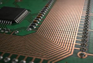
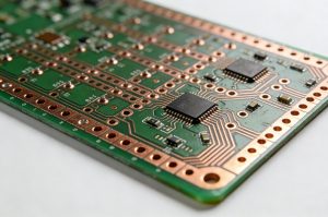
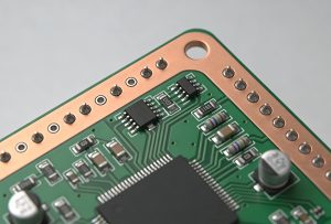
This abstract examines strategies for rigid PCB cost optimization, focusing on material selection, layer count reduction, and design simplification. It highlights how leveraging standard materials, improving panel utilization, and minimizing complexity can significantly lower manufacturing expenses. The discussion provides a roadmap for engineers to balance performance requirements with economic efficiency, ensuring cost-effective production without compromising functionality or reliability.
Read More